FOUNDRY & ENGINEERING SERVICES
Akoustis offers 150-mm MEMS based XBAW® production capabilities and engineering consulting services to meet our customers’ needs for prototype, pilot, and volume manufacturing.
Our world-class foundry provides customers unmatched bulk acoustic wave (BAW) fabrication capabilities on 150-mm Si substrates. Located just outside Rochester, New York, Akoustis’ 125,000-square-foot, state-of-the-art facility supports MEMS based XBAW® process for foundry services. Akoustis’ XBAW® technology addresses the industry’s toughest challenges with respect to power handling, co-existence, and the need for wider bandwidth filtering solutions.
XBAW® Technology
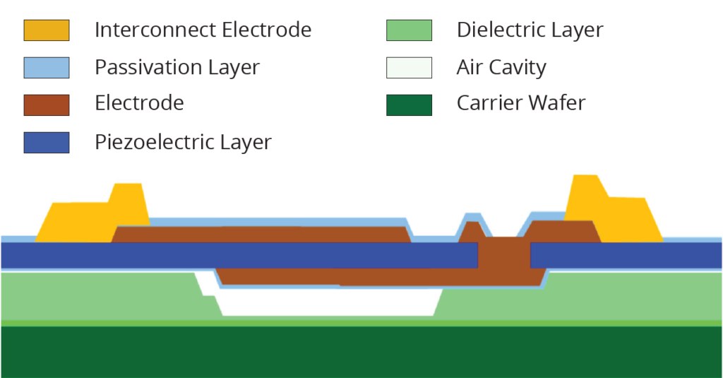
Our XBAW® technology is compatible with chip, wire-bond, wafer-level packaging (WLP) and allows design-of-experiments (DOE) to explore piezo quality influence on RF filter performance.
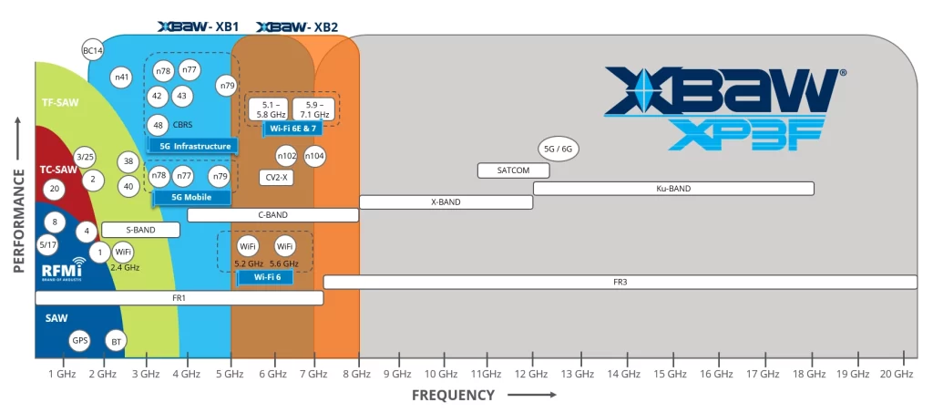
Enhanced material properties and optimized resonator FOM (k2 * Q) enables differentiated filter performance for 5G Mobile & Infrastructure, Wi-Fi, Automotive, SATCOM, and Defense applications.
| TECHNOLOGY | XBAW® (XB1) | XBAW® (XB2) | XBAW® (XP3F) |
| FREQUENCY RANGE | 1.6 GHz to 7 GHz | 5.8 GHz to 8 GHz | 8 GHz to 20 GHz Phase 2: >20 GHz |
| FRACTIONAL BANDWIDTH | 1% to 10% | 1% to 18% | 1% to 10% |
| POWER HANDLING CAPABILITY | < 4 Watts CW | < 4 Watts CW | < 2 Watts CW |
| RESISTANCE AT SERIES RESONANCE (Ω) | 0.8 | 0.5 | 0.8 |
| MIM CAPICITOR | Yes | Yes | Yes |


Process Design Kits & Models
Akoustis offers Process Design Kits (PDKs) to customers to construct designs and fabricate their end solution. The PDK provided by Akoustis utilizes AWR Microwave Office simulation design software, enabling customers to leverage advanced design and simulation tools for efficient construction and fabrication of their end solutions.
Back-end Services
GDSI serves as the driving force behind Akoustis’ back-end services, catering to customers’ advanced wafer processing needs with their expertise and reputation as a trusted and comprehensive supplier. GDSI’s services include the following:
- Wafer Dicing: Wet or dry, GDSI can develop a customized saw dicing program or apply the Stealth laser dicing process pioneered by Hamamatsu Japan
- Wafer Pick & Place: Safe chip extraction for multi-product wafer layouts. Full trace requirements with test maps or simple blind builds
- Back Grinding & Polishing: Fully automated 300mm Disco machinery designed for precision and repeatability

